Laser exposing pcb with Duet
-
Hi
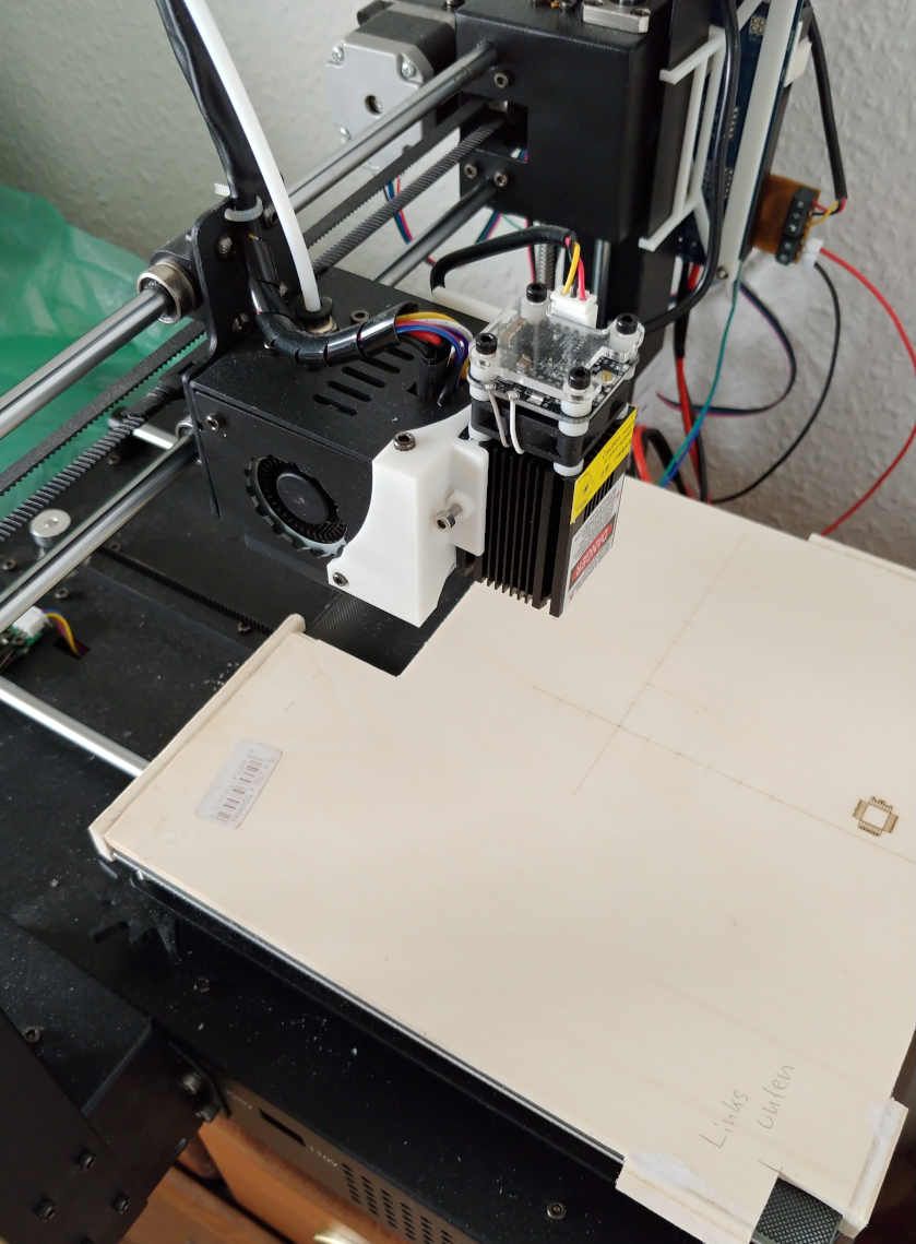
I just want to show you what can be done with a laser module and the Duet Wifi Board.
Last year I modified my Anycubic I3 Mega and ripped out its propietary brain and put a Duet Wifi in. It printed very well so my next desire was to attach a uv-laser module to it and improve my pcb exposing process and leave off the old toner transfer method.
I ordered an cheap 30€ 400nm 0.5Watt UV-Laser module and I was able to expose my photosensitive pcb's with a pwm power of 5 (of 255) and a speed of 300mm/s. This is quite slow but if I go faster I encounter a lot of jitter on small traces. So I currently can etch traces as small as 10mil (0,25mm). I did not try to go lower but I think this is still possible. Maybe its quite impractical to attach the laser to the printhead-front. That might introduce quite some mass to the construction while the head is lasering and doing rapid moves.
But the best is, the laser workflow is much less stressful and more consistent in good results.
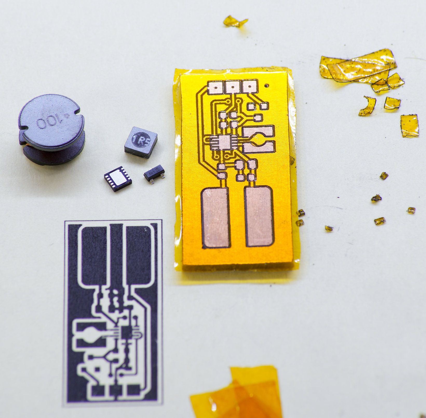
I even just tried to create a solder mask by cutting simple kapton tape, and to my surprise this worked too, with a laser power of 150 and speed 300mm/s, but with two passes.On this board (1,6x3,3cm) the big traces are 12mil. The little IC is a 3x3mm LFCSP with 0,5mm pads pitch. I have no clue if I can solder that tiny thing

So I am very pleased with the results that the Duet-Laser already delivers with even more room for optimization


PS. I use Kicad-->Flatcam to prepare my gcode files but I had to write a python script to further postprocess the gcode file from flatcam, because flatcam was made for CNC, not for laser. So I had to exchange the drill commands in the gcode with laser-on/off commands...
-
@pauledd said in Laser exposing pcb with Duet:
I even just tried to create a solder mask by cutting simple kapton tape,
you can get UV curable soldermask and it works well with UV laser. I'm also a little surprised you could cut kapton, but nice to know, thanks for sharing.
anyone wanting to try, just for the photoresist and uv curable mask you can get away with much smaller laser, I think i used 25 or 50mW wiht (negative) film and liquid solder mask.
The little IC is a 3x3mm LFCSP with 0,5mm pads pitch.
Side note that chip is probably meant to be cooled by having plated though vias in the ground plane under the thermal pad. I'd derate the chip severely or try to make the ground plane connections a lot bigger on both sides.
-
@bearer said in Laser exposing pcb with Duet:
you can get UV curable soldermask and it works well with UV laser. I'm also a little surprised you could cut kapton, but nice to know, thanks for sharing.
Do you mean this stuff:
https://www.amazon.de/gp/product/B074PTF129/ref=ppx_yo_dt_b_asin_title_o00_s00?ie=UTF8&psc=1I ordered that last year
 still wayting for arrival. But maybe my understanding is wrong but dont you need to laser expose areas which will stay on the pcb after developing? That means my laser has to scan huge areas. I cant imagine yet how I would do that.
Side note that chip is probably meant to be cooled by having plated though vias in the ground plane under the thermal pad. I'd derate the chip severely or try to make the ground plane connections a lot bigger on both sides.
You're right. Its a LDO (ADP2503) rated for 600mA with proper cooling but as I only going to draw about 20mA from that thing it should be okay.
-
@pauledd said in Laser exposing pcb with Duet:
Do you mean this stuff:
no that looks like the film used for etching.its easy to remove. the uv mask is a liquid/paste (although films are also available but I haven't found in small volumes). Yes, you'd need to scan the whole area to keep, but most non-3d-printer lasers are built to scan real fast.
flatcam can generate code to do outline + infill, but tbh its easier to export a raster and just have the laser scan across using that,
I only going to draw about 20mA from that thing it should be okay.
yeah, that ought work
-
Yes, I had rastering in my mind but as seen in normal laser engraving
graphics or logos they always seem to lack quallity, you always have artifacts of lines not touched by the laser.Well, that guy seems to use that foil for solder mask, it looks not to different...
https://www.youtube.com/watch?v=AHNv0eOq7RkDo you mean that stuff?:
https://www.youtube.com/watch?v=wvU2yyfH-XEThat looks very ugly and messy to do, especially to apply it with
a constant thickness. -
@pauledd said in Laser exposing pcb with Duet:
es, I had rastering in my mind but as seen in normal laser engraving
graphics or logos they always seem to lack quallity, you always have artifacts of lines not touched by the laser.didn't have an issue with lines, but some jagged edges due to the laser dot being oval. having flatcam do both a vector outline and a more raster style infill worked well, but fiddly to set up with multiple jobs in flatcam
Well, that guy seems to use that foil for solder mask, it looks not to different...
https://www.youtube.com/watch?v=AHNv0eOq7Rkit exist, its just hard to come by at a reasonable price. but the normal dry film is for etching as its easy to disolve, the soldermask does not come off unless you sand it off basically.
Do you mean that stuff?:
https://www.youtube.com/watch?v=wvU2yyfH-XE
That looks very ugly and messy to do, especially to apply it with
a constant thickness.Messy indeed, I ended up building a spin coater from an old harddrive, sorta worked well enough for the up to 100x70mm i've settled on using.
If I were to find the dry film soldermask at similar prices as the dry film for etching I'd drop the liquid stuff in a heartbeat.
-
Looks good!
Is your laser able to cut thin Mylar film? If so then you could use it to make a solder paste stencil. That will make it very much easier to apply solder paste to those small pads.
-
I would have thought Mylar was a no go as its transparent, but maybe not to UV after all. in any case Kapton sheets are also available.
source -
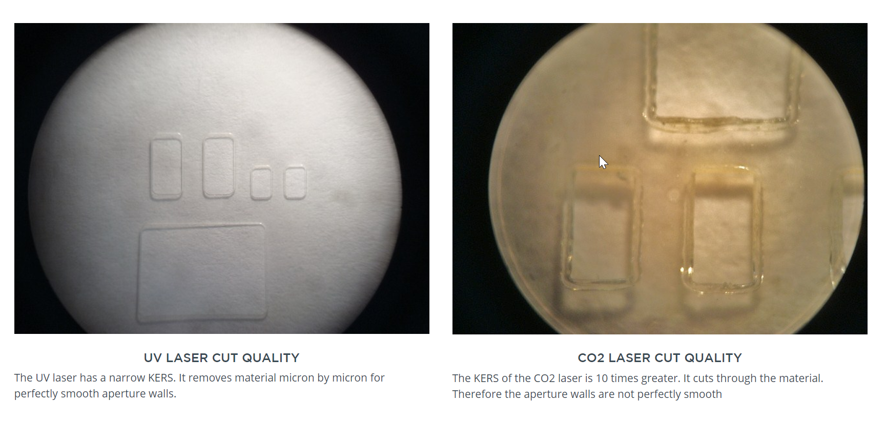
You can buy stencils laser cut from A4 transparent sheets at http://www.hobbytronics.co.uk/smt-stencils but they don't say what sort of laser they use. However, I'm not at all sure that a CO2 laser would have enough resolution. So my guess is that they use UV.
What's the wavelength of your laser?
-
OP wrote 400nm, presumably 405 or 430nm. I've used 405.
I did read a blog with someone testing CO2 for stencils and his finding was basically the same as the above, lower the power and do multiple passes for good results. But CO2 lasers are just a tad more expensive than UV, and ultimately a tad more powerful for other things as well.
I didn't think much about the above image other than to say "someone got UV working" but presumaby by KERS they meant kerf, which would limit the smallest feature and not actually have much to do with cut quality as presented. (But if you're pushing UV lasers I guess its convenient).
-
You could try this paint, but instead of the method used in the film, thin the paint with paint thinner and spray it with a paint gun on the pcb. aliexpress has complete paintgun sets complete with compressor and tank for 125 US.