Modified Laser Filament Monitor layout
-
I am working on a new extruder design that I want to be able to incorporate the Laser Filament Monitor into it but the current board layout does not work for my needs. I have modified the KiCad files and wondered if there is anyone who knows what they are doing can take a look at them and make sure that I have the layout correct. I have never done any electrical board layouts before so I am very much a novice in this.
I have decreased the overall size of the board and moved the sensor closer to the edge of the board and removed the two pin connector points that were there.
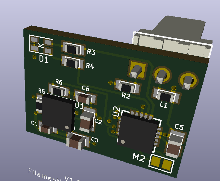
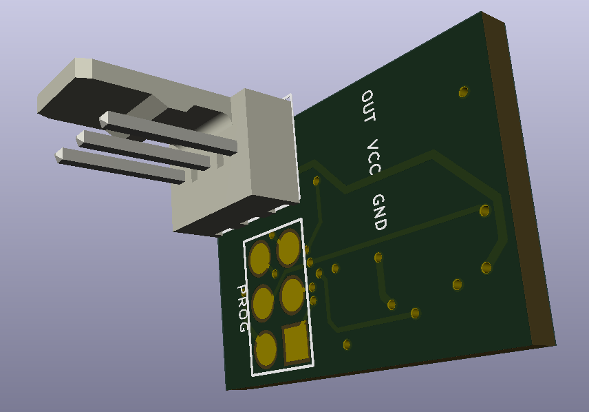
Here are a few screen shots of what I have done.
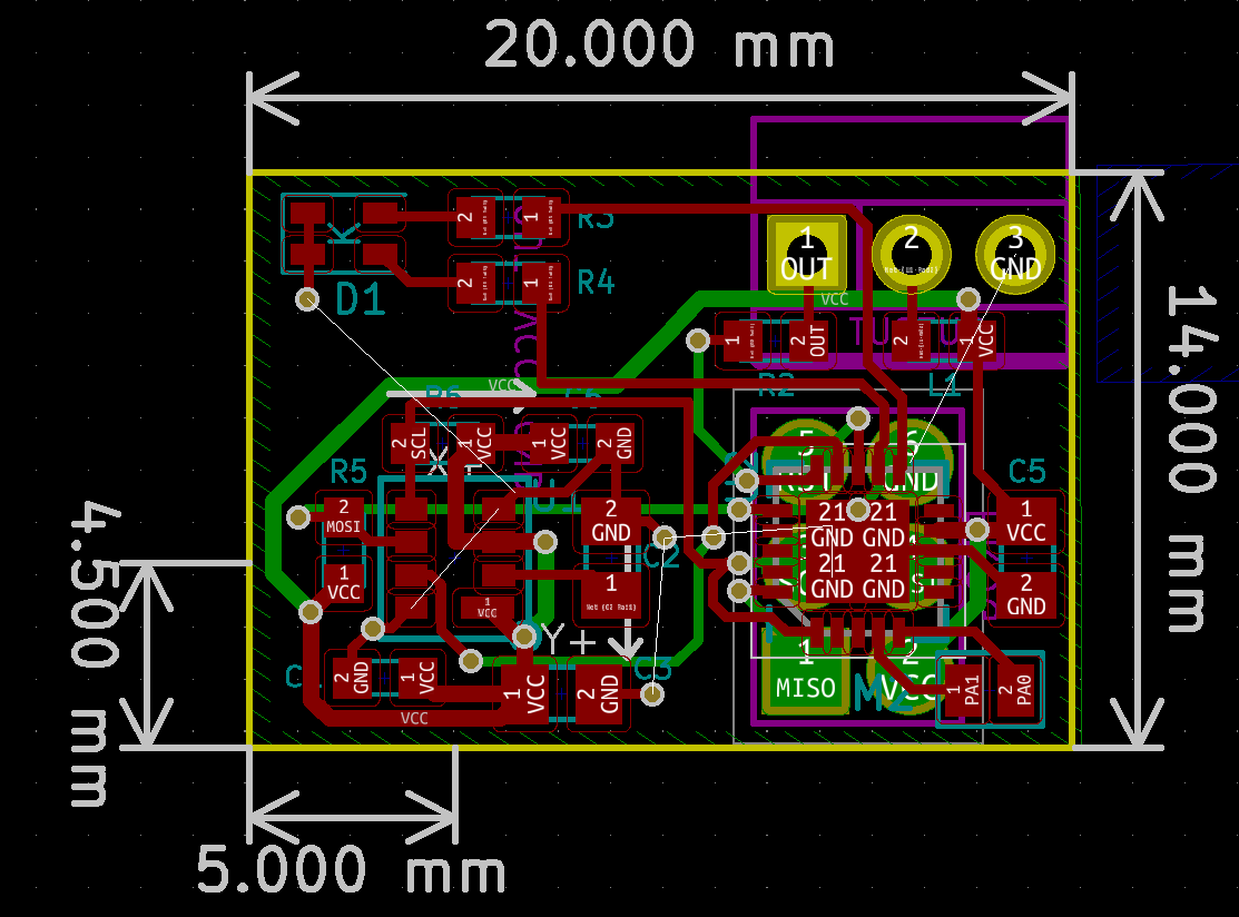
The 3D model shows the connector but I really just want the holes to solder the wires to.
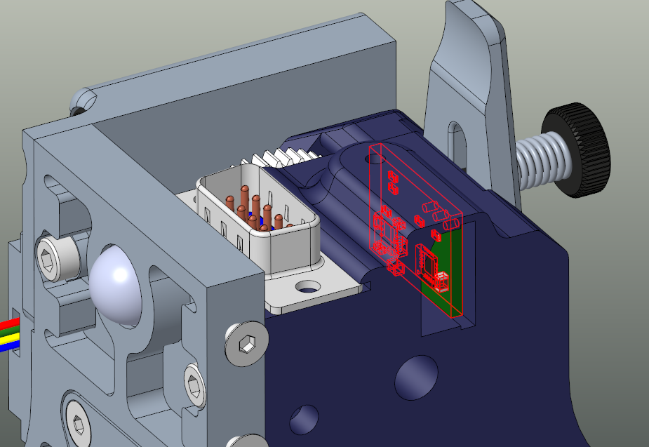
Here is a screen shot of where I am planning on putting the sensor in the extruder.
-
if you make the board from the schematic and run the design and electrical rule checks then it should be ok.
as long ad the ground plane connects all the gnd nets no major red flags at a glance.
-
Oh wow that design rule check is a big help. It found some items that were too closet together.
-
@cdl1701yahoo-com said in Modified Laser Filament Monitor layout:
It found some items that were too closet together.
have you gotten the design rules from the pcb manufacturer you intend to use? some have stricter tolerances than others. (admittedly today most are very capable)
-
Figured I would order them from JLCPCB. Got all the design rules to clear but now I am having a hard time figuring out exactly what parts to order. I figured there would be a BOM with part numbers but the BOM data does not have much information.
-
Got the PCBs ordered but so far not having much luck finding a BOM for the board. I guess if I can't find one I will just take apart the one that I have and use the parts from it.
-
your first rendering didn't show any ground planes making the missing ground connections - you did fix that with the electrical rule check right?
i haven't looked at the kicad sources, but aren't the part designators on the schematic at least, even if lacking supplier data?
-
Yes, I got the missing grounds fixed and there were also some VIAs that were too close to traces so I got all those fixed.
As for the BOM here is what it looks like. For example the 470R resistor on Mouser there are a bunch to choose from how do I know what I should use. Also the sensor I cannot find where to actually purchase it. It could be that I just don't know much about what I am looking at.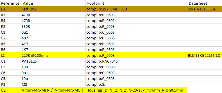
-
ah, yeah, it seemed the manufacturer only have two distributors for their sensor and not using digikey/mouser/etc, not sure if its easy get a hold of a one-off. if you go with the plan to scavenge parts of another board pay attention to the solder temp and times listed for the sensor.
as for the passive components, unless there is a note on the schematic just pick the cheapest with the correct resistance and footprint. if there are special conciderations like tolerance, power rating or temperature coefficients its usually noted somewhere. like you see the inductor specifies 100Mhz.
Part Number
PAK9125LP-xxxxWhere to Buy
North America:WPG America (Distributor)
Website: http://www.wpgamericas.com/contact-us/
Taiwan and China:
AIT Group (Distributor)
Website: http://www.wpgholdings.com/aitg/pline_detail/en/PixArt